Converting secondary materials from electronics into precious metals at Harjavalta
Boliden’s Harjavalta smelter in Finland is working to optimize its recovery of precious metals from secondary materials from electronics through ongoing R&D.
The Harjavalta smelter on Finland’s west coast is one of the most efficient copper and nickel producers in the world. Harjavalta sources concentrates from a number of mines, including Boliden’s Kylylahti and Kevitsa mines in Finland, and adds secondary materials from electronics to its feed to recover precious metals contained in waste.
Processing secondary materials from electronics
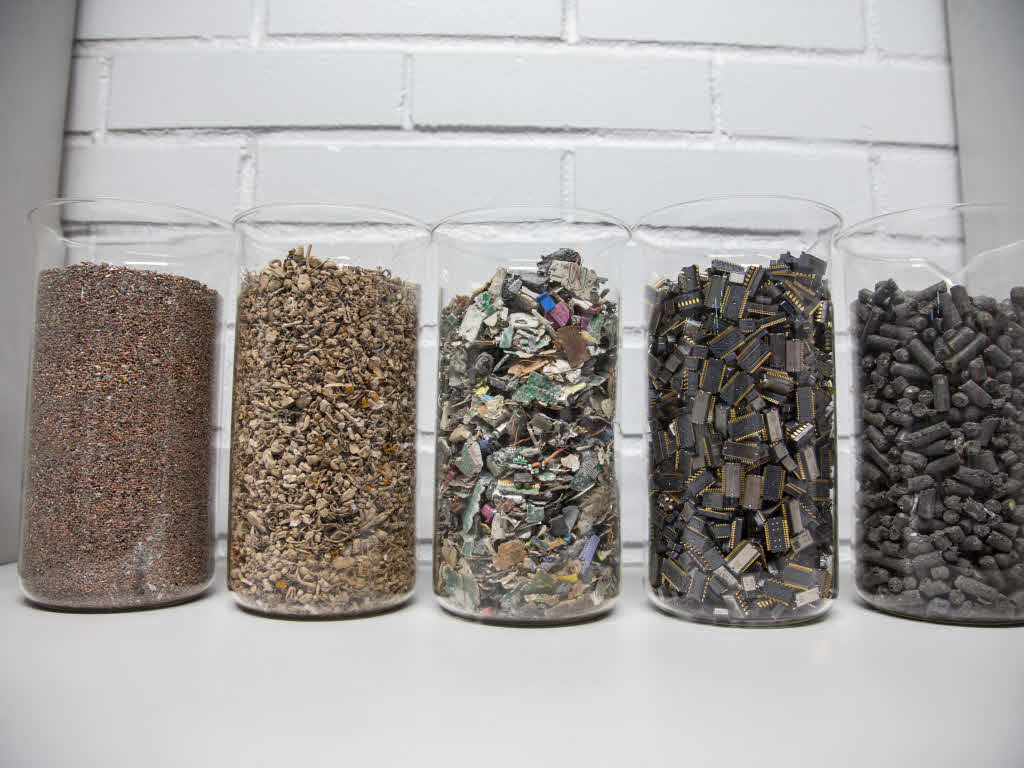
The Harjavalta smelter annually sources and processes almost 10,000 tonnes of secondary materials from electronics. The secondary materials arrive at the smelter as pre-crushed pieces that are between 10 to 30 mm in diameter from various sources in Finland and abroad.
Secondary materials from electronics are added to the Harjavalta copper line and are smelted together with copper concentrate. “In the last couple of years, we have managed to increase the proportion of secondary materials from electronics we can include in our smelter feed,” explains Petri Latostenmaa, R&D Manager at Harjavalta. “This has been done through investments and the refinement of the feed process.”
Value from discarded materials
“We produce between 1,000 and 2,000 tonnes of copper from secondary materials from electronics each year, along with quantities of precious metals such as gold and nickel,” says Latostenmaa.
The plastic in the secondary materials from electronics is combusted in the smelting process to generate heat, which is recovered and used to dry concentrates or delivered to other industrial partners in the area. All the gases from smelting are treated in a sulphuric acid plant and emissions to air are minimized.
More circular resource use in society
Smelters such as Harjavalta play an important role in contributing to a more sustainable and circular society by enabling the recycling of electronic materials. They also help European member states achieve their waste targets such as the European WEEE (Waste Electrical and Electronic Equipment) directive on waste electrical and electronic equipment, and support the Restriction of Hazardous Substances (RoHS) Directive.
Further improvement through Research & Development
Latostenmaa, who heads the R&D team at Harjavalta, which works closely with Boliden’s other smelters and the Group experts to share knowledge and experience says: “This knowledge sharing we have within Boliden is incredibly important for further improving our processes and optimising the value we can recover from waste such as secondary materials from electronics, and for finding new commercial uses for waste products.”
“This cooperation includes working with universities and other partners to develop and scale up innovative secondary materials from electronics recovery techniques,” says Latostenmaa. “We are looking into ways of reusing slag after the smelting of concentrates and secondary materials – for example by making it more stable so it can be used as a geopolymer in construction applications.”